
Explained: China Attains Key Breakthrough In 7nm Semiconductor Space
- InduQin
- Aug 18, 2022
- 4 min read
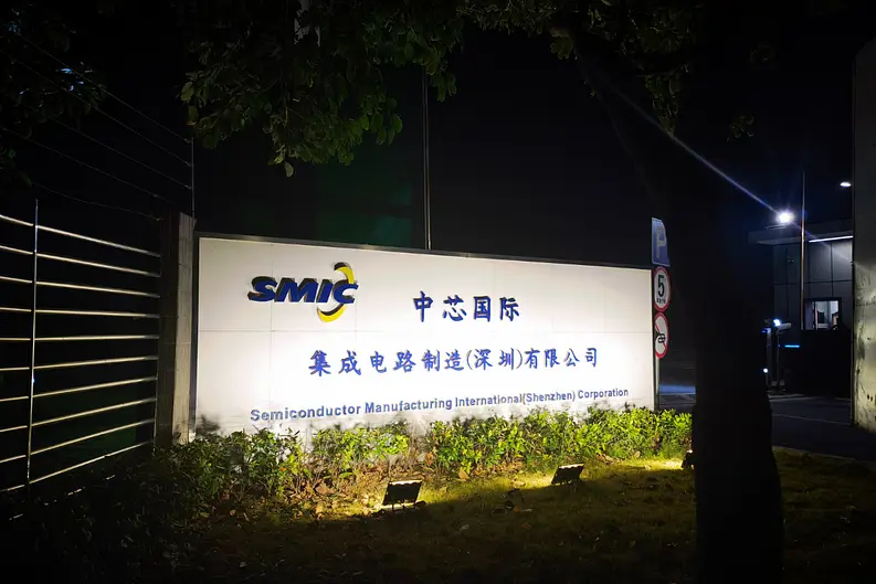
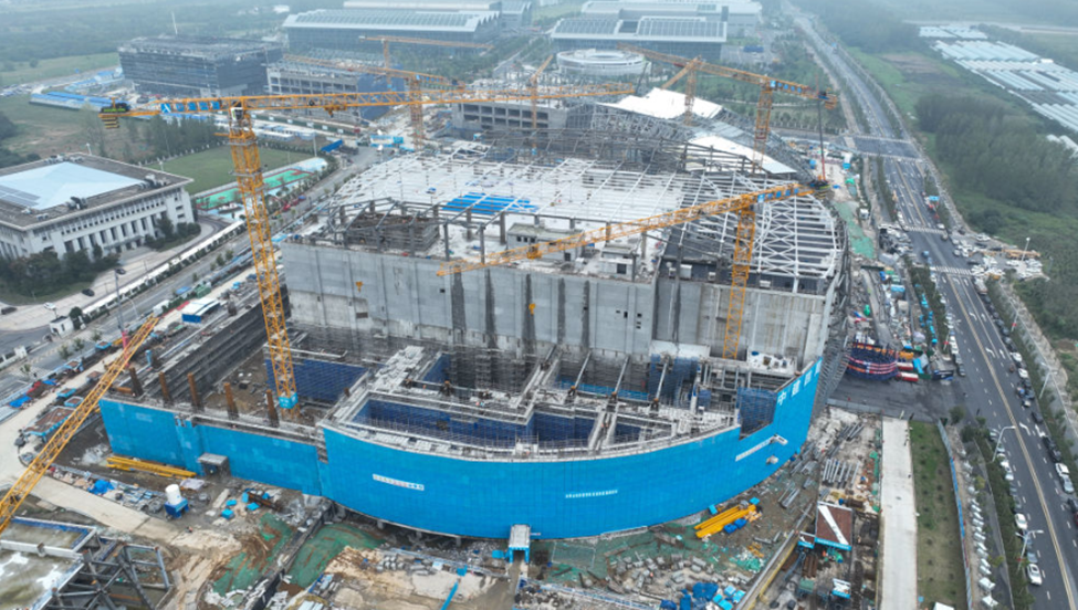
SMIC, the Chinese flagship semiconductor company, is learnt to have become capable of making chips using the 7 nm technology.
Context: Only Taiwan's TSMC and Korean electronics giant Samsung were known to have mastered the art of using 7 nm technology to make chips.
- Intel and other industry leaders are said to have struggled. Some even abandoned efforts towards the 7 nm effort.
- “SMIC, China’s largest foundry, has slowly been catching up to TSMC, Samsung, and various western foundries in process technology,” an analyst said.
- “They are rapidly approaching (the) position as the world’s third largest foundry and have higher margins than the current number 3, GlobalFoundries,” he added.
Background on ‘7 nm’: Manufacturing chips on an industrial scale involves printing patterns from templates (photomasks) on to a substance called photoresist, coated on top of wafers that are mostly made out of silicon.
- Photoresist is a substance that hardens or softens based on where light falls on it (or does not).
- The softened or hardened part can be selectively removed by a process called 'developing' and through that "opening" you can perform various functions — for example, introduce foreign substances ("doping") or dig up ("etch") the silicon below that opening to a certain depth and then sometimes filling that opening with metal ("deposition") and so on.
- The whole process is called fabrication, and the facility where it is done is called a 'fab'.
From photomasks to chips: A chip may contain many layers of patterns ‘printed’ using photomasks and many other processes.
- Usually, transistors are stacked horizontally with some bit of variety in their size and features; this needs a few templates or photomasks.
- Further photomasks are needed to make the electrical connections.
- The process of printing the pattern from the template (photomask) to the photoresist is called photolithography or sometimes simply lithography or even just litho.
“Step and scan” litho: The photomask in itself is a piece of glass on which the pattern is printed (template) using substances that have certain properties, such as chromium.
- The template must be as close to perfection as possible; making it (writing) is a slower process compared to using it for mass printing.
- “Step and scan” is the most commonly used tool for photolithography.
- It is called 'step and scan' (or stepper/scanner) because in each exposure, a source of light scans the area of the template and once one die is done, it steps and exposes the next die on the same wafer.
How small can your templates and printing get? It depends on the wavelength of the source of light used in the photolithography tool — in this case, the step and scan.
- Lower the wavelength, smaller is the feature size than can be printed.
- Usually laser-produced ultraviolet (UV) light is used. UV has wavelength lesser than visible light; examples are 365 nm, 248 nm, and 193 nm.
- 193 nm wavelength falls in the "Deep UV" (DUV) category.
- Using step-and-scan tools of 193 nm wavelength source, printing the smallest features in the design of a 90 nm technology node chip was relatively easy.
- Up to about 65 nm or perhaps even 55 nm chips are possible with certain optical correction tricks. - Wavelength below 193 nm started falling into the extreme ultraviolet regime (EUV) and then there was a big challenge — this light is absorbed by glass and even by air.
Litho gets into EUV. For EUV to be effective, the whole system has to be in a tight vacuum, photomasks have to be reflective, and, instead of a lens system, you need a projection system based on extremely smooth mirrors.
- Developing such a system impacted another key factor involved in the lithographic process, called the numerical aperture (NA).
- NA is a measure of the amount of light captured by the projection system and sent to the photoresist-coated wafer.
- Higher the NA, better is the ability to print smaller features.
- While the 193 nm tool had an NA of nearly 1, the EUV tool at present mostly has an NA of only 0.33 (the one with 0.55 has just started to come out).
- Therefore, in order to get a significant benefit in using EUV, the wavelength has to be much smaller than 193 nm.
- Eventually, a 13.5 nm EUV source is what the industry zeroed in on.
Industry found a shortcut with 193 nm source: A layer of water was added between the projection lens and wafer to achieve an NA close to 1.35. This came to be called immersion lithography. It made 28 nm possible — perhaps even 22 nm with some other tricks.
- Below that, for those layers with the smallest features, industry started doing "multiple patterning." - Imagine that you want to print a ‘feature’ of 10 nm. But the smallest your lithography tool can achieve is a 20 nm feature.
- By using a photoresist and developer combination, and by shifting the mask by 10 nm, you can achieve 10 nm etching.
- This is a simplified explanation. The process is more complicated.
- The industry achieved 16/14/12 nm, even 10 nm technology node, with multiple patterning.
But how about 7 nm? To achieve 7 nm, complicated versions of multi patterning had to be employed and the risk of failure was more.
- Meanwhile, EUV-based step-and-scan tools started becoming available and foundries like that of Samsung started using that for its 7 nm process.
- TSMC was also successful with multi patterning at 7 nm, while Intel struggled and GlobalFoundries eventually dropped their efforts.
Takeaway: SMIC was seen as stuck at 14 nm for a long time. However, the latest news indicates that the Chinese foundry too has managed to make 7 nm chips using DUV and multiple patterning — a notable technological achievement for the Chinese semiconductor industry.
Read More at https://swarajyamag.com/context/explained-china-attains-key-breakthrough-in-7-nm-semiconductor-space


Comments